Besides research, microscopic analysis is also applied for quality control and defect analysis. It shows the correlation between structures of polymers and their mechanical properties. In addition, microscopic analysis is important for understanding the influences of processing parameters on materials and their mechanical failures.
Thin sections of thermoplastic polymers are prepared by microtome for some microscopic analysis using transmitted light. For very soft materials, the cooling of specimens is important. Samples can be embedded in acrylic resin for long-term storage the specimens. Reinforced polymers can be first embedded in epoxy resin and then be polished. Samples for SEM will be sputter coated with a gold, platinum or chromium layer to avoid charging.
Depending on different illumination systems, there are transmitted-light and reflected-light microscopes.
- In transmitted light microscopy, the light passes through the section and then be captured by the objective. Therefore, transparent thin sections are needed.
- In reflected-light microscopy, illuminating light reaches the specimen, which may absorb some of the light and reflect some of the light, either in a specular or diffuse manner. Light that is returned upward can be captured by the objective in accordance with the objective’s numerical aperture.
| Transmitted light | Bright field | Impurities |
|---|---|---|
| Polarization | Spherulite structure, orientations | |
| Phase contrast | Polymer blends | |
| Reflected light | Bright / Dark field | Impurities, cracks |
| Differential interference contrast | Fiber distribution | |
| Fluorescence | Cracks |
- Due to its large depth of field, the scanning electron microscope is preferred for imaging unevenly structured surfaces.
- For the material identification of microscopic samples, energy dispersive X-ray microanalysis (EDX) is used in the SEM to detect elements and their distribution.
- Industrial computed tomography (CT) is used to analyze the internal structure of components without contact and without causing damage. Classic applications include porosity and void analysis, target/actual comparison (deviations in the shape of the model and component), and non-destructive wall thickness analysis.
For sample preparation
| Device | Device data | Aim |
|---|---|---|
| Grinding/polishing equipment | Water-cooled | Preparation of ground sections; Surface treatment |
| Sled microtomes, rotary microtomes | Cutting thickness: material-dependent (min. 3 µm); Freezing device | Thin section preparation; Surface treatment |
| Precision cutting machines | Cutting discs: 75-203 mm; Water-cooled | Fast and precise cutting of workpieces |
| Saw microtomes | Cutting thickness: 100 µm to 1 cm; Sample size: 25 mm diameter; 30 mm height | Production of plane-parallel cuts of samples |
| Plasma etching system | Microwave-generated plasma; Chamber volume: 43 liters; Gas: O₂, He, Ar | Physical etching |
| Sputter coater system | Layer thickness: 0.5–2 nm; Target materials: Au, Pt, Pd, C | Metallic, conductive coating of the sample surface for SEM examinations |
For microscopic analysis
| Device | Device data | Aim |
|---|---|---|
| Light microscopes (reflected light microscopy) | Magnification: 25 to 1000x; Bright field, dark field, and polarization contrast; DIC and C-DIC contrast; Fluorescent lamp; Digital image capture | Examination of ground sections; Optical representation of: fillers and reinforcing materials, defects, and material deformations |
| Light microscopes (transmitted light microscopy) | Magnification: 25 to 1000x; Bright field, polarization, and DIC contrast; Phase contrast; Tilt compensator B (5); Digital image capture; Heating table device | Examination of thin sections; Optical representation of: material structure, defects, and particles |
| Stereomicroscope (transmitted light and reflected light microscopy) | Magnification: 5 to 150x; Transmitted light: Bright field and polarized contrast; Oblique light; Reflected light: Bright field contrast, oblique light | Surface analysis; Spatial observation of objects |
| Large-area optical stress tester | Field of view: 300 mm; Linear and circularly polarized light | Determination of residual stresses and orientations |
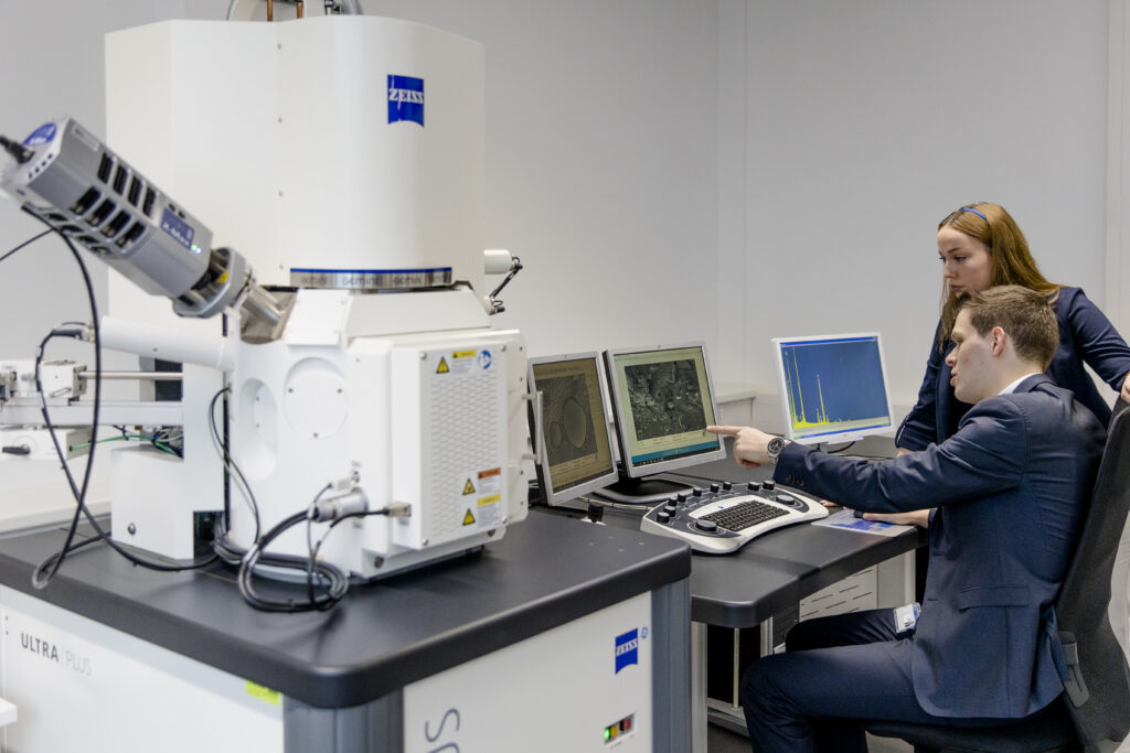
| Canning electron microscope | Magnification: 20 to 150,000x; secondary electron and backscattered electron detector; digital image capture; EDX system | Structure and fracture surface analysis; Element analysis |
| Computed tomography system (Sub-µCT) | Detail recognition: from 500 nm; Max. object size: 65 mm diameter; Max. voltage: 160 kV | Non-destructive and three-dimensional examination of components |
The Institute of Polymer Technology organizes seminars with practical demonstrations and symposias on selected topics regularly. An overwiew of the currently planned events can be found on here.
Contact person
Dipl.-Ing. (FH) Gabriela Riedel
Institute of Polymer Technology
- Phone number: +49 9131 85-71069
- Email: gabriela.riedel@fau.de